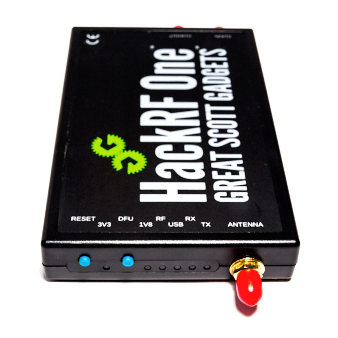
The HackRF One is a test equipment module for RF related experiments and measurements which covers a frequency range from 10 to 6000 MHz. It is used for experiments and measurement setups with open source programs for SDRs, own software development for radio communications and measurements in amateur radio. The hardware was developed by Michael Ossmann (USA) as an open source device, backed by a strong Kickstarter funding project. It is now sold as a commercial product as well.
The system covers a wide frequency range from 10 to 6000 MHz, and covers many licensed and unlicensed as well as ham radio bands. The hardware offers a maximum sample rate of 20MS/s, which is sufficient to measure even wide band signals like WFM, DECT, Wifi and others. The ADC works with 8 bit data width and offers a dynamic range of 48dB. The digitised I/Q data is handled by a Xilinx CPLD and an integrated ARM Cortex processor. Due to the design and component selection the device supports only half-dulplex operation.
The entire circuitry is designed for low power consumption, supply is done over USB only. The board has a Micro-B USB socket, a suitable cable is included. To synchronise several HackRF One boards, the system offers connectors for clock input and output. These signals can be used to use multiple boards in parallel, for example for measurements on MIMO systems or full duplex systems. Two push buttons and several diagnostic LEDs are provided for easy operation.
The PCB is professionally manufactured with 4 layers. All components are SMD parts. To support own hardware development and extensions, many signals are available on jumper sockets. These connectors offer GPIO pins as well as parameter in- and outputs from the CPLD. A JTAG connector can be used to program the ARM Cortex processor.
HackRF One Circuit Description
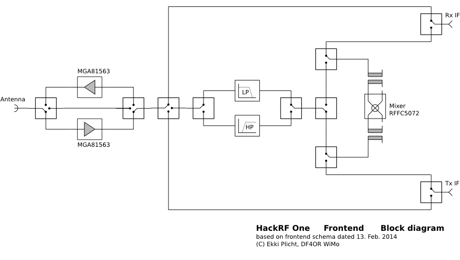 HackRF 1 Block Diagram FrontendZoom HackRF One Frontend Block Diagram
Please refer to the frontend block diagram. The HackRF One board is characterised by a very high flexibility when choosing the signal path. RF switches at all critical junction points allow the selection of various components, based on user programming.
After the antenna input two MGA-81 GaAs MMIC amplifiers follow, one serves the input, the other the output path. The amplifiers ICs can be selected in and out of the signal path by RF switches (SKY13317).
The amplifier block is followed by a low-pass and a high-pass filter, which can be used to limit the signal in either path (input/output). After the filter the signal arrives at an RF mixer RFFC 5072. This mixer can be used up to 6GHz. The signal is mixed up or down, depending on user programming and finally fed to the baseband circuitry. Mixer and filters can be bypassed by further RF switches, allowing the IF signals to be switched directly to the amplifiers or directly to the antenna.
As baseband chip a Maxim MAX2837 component is used, which covers a frequency range of 2.3 to 2.7 GHz. The chip uses monolithic filters which provide for a very linear signal and a low noise figure. The IQ data is then passed to an ADC/DAC chip Maxim MAX5864. This ADC as well as the DAC uses has 8 bit resolution. A maximum sample rate of 20MS/s is supported by these converters. The digital signals are finally passed to a Xilinx XC2C CPLD. The entire system and all interfaces are controlled by a powerful ARM Dual Core Cortex processor (NXP LPC4320). The board further supports 1MB flash memory.
Software for the HackRF One Board
 Currently (Autumn 2014) the HackRF One board is working with ‘SDR-Radio’, ‘GNU Radio’ and ‘SDR#” (SDR Sharp). Due to the open source and license fee free nature of the project, other software project can join at any time. Several authors already have announced their support for the HackRF One. Up to date information about software is found on the manufacturers Wiki site.